a2fpga-series — Part 1
The Card That Made the Apple II Serious
The Videx VideoTerm was the 80-column card that turned the Apple II into a business machine. Emulating it on an FPGA means reverse-engineering a 1981 MC6845 CRTC design and understanding why slot 3 is unlike every other slot in the machine.
Part 1 of 2. This part covers the Videx VideoTerm’s hardware architecture, the MC6845 CRTC, and why slot 3 is architecturally special. Part 2 covers the rendering pipeline, C8 ownership, and the Pascal boot hang.
In 1977, the Apple II shipped with 40 columns of text. That was fine for BASIC programs and games. It was not fine for WordStar, VisiCalc, or the CP/M business software that was reshaping the industry. A serious word processor needed 80 columns. A spreadsheet with real data needed 80 columns. Anyone who wanted to use an Apple II for actual work needed 80 columns.
The Videx VideoTerm, introduced in 1980 and manufactured in Corvallis, Oregon, was the card that solved this problem — and dominated the market until Apple built 80-column support into the IIe in 1983. It was the most widely supported 80-column card for the Apple II and II+, compatible with Apple Pascal, WordStar, and virtually every serious business application of the era. Understanding why it worked the way it did requires understanding a chip that has largely faded from memory: the Motorola MC6845 CRT Controller.

The Display Problem
Before getting to the Videx card itself, it helps to understand what Apple II video actually looked like.
The Apple II+ outputs NTSC composite video — a single analog signal designed for 1970s consumer televisions. It works, in the sense that you can see the screen. But NTSC composite has color bleeding, chroma artifacts on text, and a horizontal resolution that is fundamentally limited by the bandwidth of the signal. The 40-column text mode that the stock Apple II produces is legible on a period-correct TV. On anything else it is a reminder of how much display technology has changed.
The A2FPGA bypasses composite output entirely. Rather than capturing and upscaling the analog signal, it monitors the Apple II’s video memory — the text pages and hires graphics pages that the Apple II’s video circuitry reads to generate its composite output — and generates HDMI directly from those memory contents. The FPGA reads the same bytes the Apple II would use to build its composite signal, and renders them into a clean 720×480 digital frame. The result is text and graphics at correct pixel boundaries, with no analog smear.
Adding the Videx emulation extends this pipeline. The Videx card has its own 2KB of video RAM, separate from the Apple II’s memory map, that stores the 80-column character grid. When 80-column mode is active, the FPGA substitutes its Videx VRAM rendering for the Apple II’s native 40-column text — producing sharper 80-column output on a modern HDMI display than any physical Videx card connected through the Apple II’s composite output ever produced.
The MC6845
The MC6845 is a programmable CRT controller from 1977. Its job is to generate the timing signals that drive a CRT display: horizontal sync, vertical sync, and cursor position. It is not a video chip in the modern sense — it generates no pixel data itself. It tells the host system where the electron beam is and trusts the host to supply the right character data at the right time.
The 6845 exposes 18 registers through a two-port interface. You write a register number to the address register, then read or write the data register. The registers control everything from the number of characters per line to the vertical total to the cursor blink rate. The registers are largely write-only on the original MC6845, though the Hitachi HD6845SP used on the Videx VideoTerm is a Type 1 variant that allows full read-back — a detail that matters for software that checks its own configuration.
If you look at the physical Videx board, the HD46505SP is the largest chip, front and center. The two 2716 EPROMs above it — labeled “INVERSE (C)1981 VIDEX” and “STD. 7X9 E (C)1981 VIDEX” — are the two halves of the character ROM. The “VI-FIM-500 (C)1982 VIDEX” chip is the firmware ROM. A small army of 74LS-series logic chips handles address decoding, bus buffering, and timing.
The FPGA emulation replaces all of it. Every chip on that board — the HD46505SP, both character ROM EPROMs, the firmware ROM, and all the glue logic — lives in about 250 LUTs and 160 registers in the GW2AR-18C fabric.
Why Slot 3 Is Different
The Apple II has 7 expansion slots. Electrically, they are almost identical — each provides the same set of bus signals plus a slot-specific I/O select and device select. But slot 3 has a hardware quirk that makes it unlike every other slot in the machine: it controls the INTCXROM internal ROM mechanism.
When the CPU accesses memory in the $C300–$C3FF range (the slot 3 ROM space), the Apple II hardware checks a soft switch called SLOTC3ROM. If SLOTC3ROM is 0 (the default), accessing $C300 sets a flag called INTC8ROM, which routes the $C800–$CFFF expansion ROM space to the Apple IIe’s internal 80-column firmware instead of external cards. On the Apple ][+, SLOTC3ROM doesn’t exist, so it’s always 0 — meaning any $C3xx access would set INTC8ROM and block all expansion ROMs from every card.
This is why Videx must be in slot 3. The SLOTC3ROM/INTCXROM mechanism exists specifically for the 80-column card slot. The Videx firmware is written to work within this constraint — it accesses $CFFF at specific points to release C8-space ownership and let other cards’ expansion ROMs operate. The slot 3 hardware architecture is, in effect, the 80-column card architecture baked into silicon.
Emulating this correctly means understanding the ownership protocol, which turned out to be one of the more subtle parts of the implementation.
The Address Map
The Videx card responds to three address regions:
$C0B0–$C0BF (device I/O) — This is the slot 3 device select range. Address bits [3:2] select one of four 512-byte VRAM banks. Address bit [0] selects between the MC6845’s address register (even) and data register (odd). Writes go to the CRTC. Reads return CRTC register values or VRAM contents.
$C300–$C3FF (slot ROM) — The 256-byte slot firmware ROM. Accessing this range also sets the expansion ROM ownership flag, giving the Videx card control of the $C800–$CFFF space.
$C800–$CFFF (expansion ROM + VRAM window) — Once the card owns C8-space, it serves its 2KB firmware from $C800–$CFFF. Within this range, $CC00–$CDFF is a VRAM window: the 512 bytes of VRAM currently selected by the bank bits in the device I/O address.
The VRAM window is clever. The Apple II’s video RAM on the Videx card needs to be 2KB (80 columns × 24 rows = 1920 bytes, rounded up). But the slot ROM is only 256 bytes and device I/O is only 16 bytes. The expansion ROM space is 2KB — and by carving a 512-byte window into it at $CC00, the Videx firmware can access the full VRAM through the C8 space, bank-switching between four 512-byte pages via the device I/O address bits.
The Firmware ROM
The Videx firmware is a 2KB ROM that serves two address ranges: the 256-byte slot ROM at $C300 and the full 2KB expansion ROM at $C800. It contains the Apple II character output hook, the 40/80-column switching logic, and interrupt handler patches.
The key entry point is at $C300, where the first two bytes are $2C $CB — a BIT $CBxx instruction. This is the standard Apple II slot ROM idiom: the first byte is a BIT opcode, which executes harmlessly but uses the next two bytes as an address operand. This lets the firmware signal to the system that this ROM has a Pascal-compatible entry structure, and it allows CALL 771 (which is $C303) to be a valid Pascal peripheral card protocol entry point.
$C313 contains 4C 00 C8 — JMP $C800 — which hands control to the expansion ROM for the main initialization path.

That CardCat screenshot is reading $C300–$C3FF directly from hardware. It has no knowledge of the A2FPGA — it’s a generic ROM examination utility. The bytes it returns match the original Videx firmware exactly, because that’s what the emulation is serving.
The VRAM Architecture
The Videx VideoTerm uses 2KB of video RAM to store the 80×24 character grid. In the original hardware, this is implemented as static RAM with dedicated address multiplexing between the CPU and the MC6845’s display scan. The 6845 reads character codes sequentially as it scans the display, while the CPU writes new character data through the device I/O window.
In the FPGA implementation, the 2KB VRAM is a single Gowin SDPB block — a simple dual-port block RAM with asymmetric port widths. The write port is 8 bits wide (CPU access through the $CC00–$CDFF window). The read port is also 8 bits wide and connects to the rendering pipeline’s character lookup logic.
The bank addressing scheme maps cleanly: the device I/O address bits [3:2] select which 512-byte bank the $CC00–$CDFF window points to, giving the firmware access to all 2048 bytes of VRAM across four bank accesses.
The Character ROM
The Videx character ROM stores the pixel patterns for each character: 256 characters, each 16 rows tall (though only 9 rows are active in the standard 7×9 font), 8 pixels wide. In the original hardware, that’s two 2KB EPROMs — which is why the physical card has two chips, labeled “STD. 7X9 E” (the standard character set) and “INVERSE” (the inverse video characters $80–$FF, which are simply the bit-inverted versions of characters $00–$7F).
In the FPGA, storing both halves would cost 2 BSRAM blocks (pROMs) for 4KB of data. But the inverse relationship is exact — character $80 is character $00 with every pixel bit flipped — which means we can store only the lower 128 characters and generate inverse pixels in logic. One XOR gate per pixel, triggered by bit 7 of the character code. This saves one full BSRAM block, which matters: the GW2AR-18C has only 46 BSRAM blocks total, and the complete five-card build uses 45 of them.
The implementation uses only the low 7 bits of the character code for the ROM address, then XORs the output with a mask derived from bit 7 and the cursor active signal:
// ROM lookup uses only low 7 bits (128 unique characters)
videxrom_a_r <= {char_code[6:0], scan_line[3:0]};

// Inverse and cursor combined into a single XOR at pixel capture
pix_buffer_r[6:0] <= videxrom_d_r[6:0] ^
    {7{videx_data_r[7] ^ (cursor_active && cursor_byte == 2'd0)}};
The cursor blink and inverse video merge into a single operation. On real Videx hardware, cursor inversion and character inversion are separate mechanisms implemented with discrete logic. In the FPGA, they collapse to one XOR.
Proof of Identification
Software that knows how to identify expansion cards will find exactly what it expects:
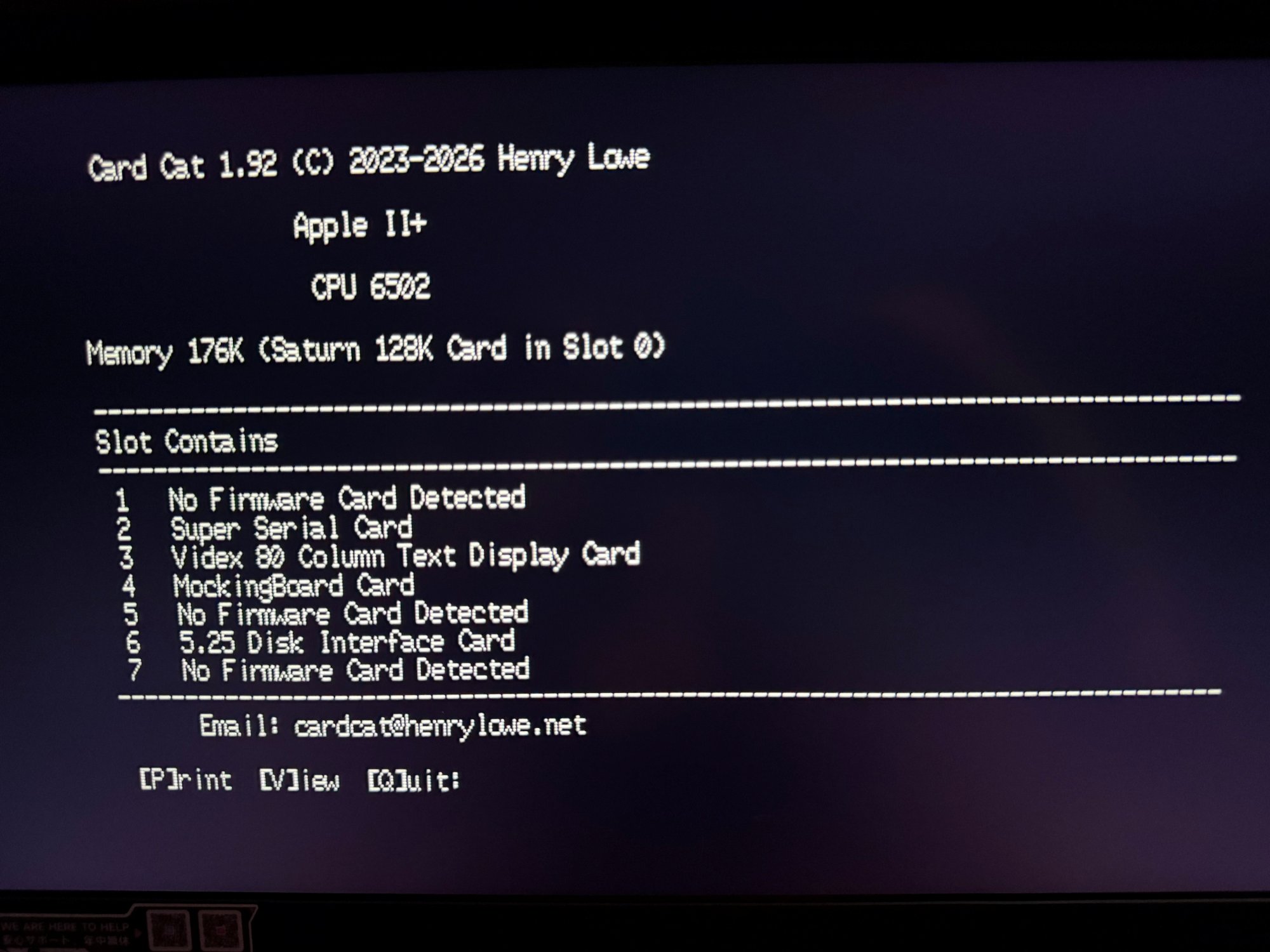
CardCat reads the firmware ROM signature bytes from each slot and matches them against a database. Slot 3 comes back as “Videx 80 Column Text Display Card” because the firmware ROM bytes are identical to what a real Videx card would return. The emulation is indistinguishable from hardware to software that doesn’t know to look for an FPGA.
Part 2 covers how the character data gets from VRAM to pixels on the screen: the rendering pipeline, the C8-space ownership state machine, and the Pascal boot hang that took the longest to diagnose.